Semiconductor
Precision in Semiconductors
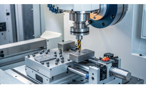
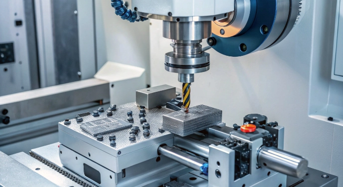
In the world of semiconductor manufacturing, precision isn't just nice to have; it's essential. CNC precision machining plays a vital role in achieving the level of accuracy required to make the miniature marvels we rely on every day. Let's dive into why this process is so crucial and how it's applied.
The Need for Precision
Semiconductors are the heart of modern electronics, and their performance hinges on precision at the microscopic level. CNC machining center helps by:
Offering tolerances down to a few microns, vital for the minute parts within semiconductors.
Providing consistency across mass production, ensuring every component performs as expected.
Enabling the creation of complex geometries needed for sophisticated designs like MEMS.
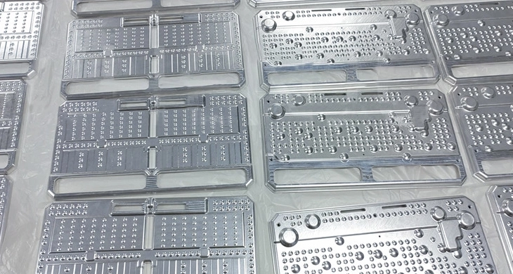
Applications in Production
Here's where CNC precision machining shines in the semiconductor industry:
Wafer Fabrication: Ensuring silicon wafers are cut and shaped with uniform thickness for flawless photolithography.
Die Attach and Wire Bonding: Precision placement of dies and bonding of wires, critical for chip assembly.
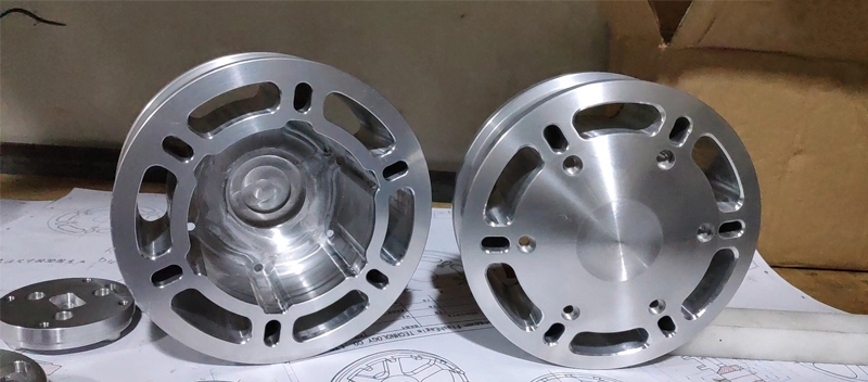
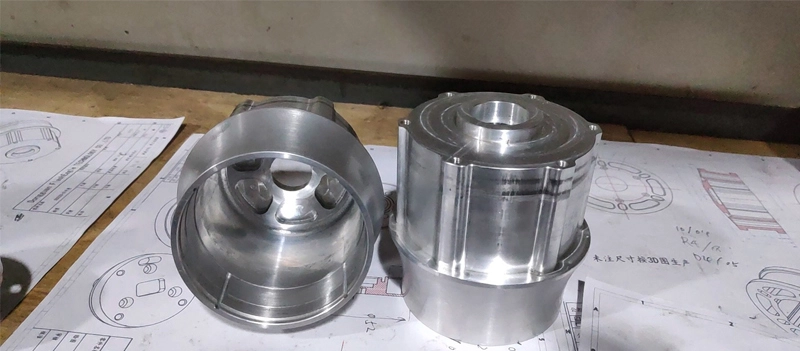
MEMS and Packaging: Crafting the intricate features needed for micro-electromechanical systems and housing delicate semiconductor components.
Materials and Methods
Silicon and ceramics make up the bulk of machined materials in semiconductors. Here's how they're handled:
Material Challenges
Silicon, though brittle, is machined with great care for surface quality. Ceramics, used for their thermal properties, require precision to shape into functional components.
Machining Techniques
CNC Milling: For creating detailed surfaces and features on semiconductor parts.
CNC Turning: Used for cylindrical parts, ensuring precise diameters and finishes.
Precision Drilling: For exact hole placement and size in semiconductor substrates.
| Technique | Application in Semiconductors |
|---|---|
| CNC Milling | Complex surface creation on wafers and chips |
| CNC Turning | Accurate shaping of cylindrical components |
| Precision Drilling | Creating micro-holes for connectivity |
Overcoming Industry Challenges
Dealing with Material Sensitivity
Semiconductor materials can be finicky, requiring specialized tools and meticulous control over cnc machining conditions.
Maintaining Tight Tolerances
As devices shrink, the need for precision only grows, pushing for constant innovation in machining tech.
Clean Environment
Cleanroom conditions are a must to prevent even the tiniest particle from ruining a batch, demanding CNC machines with minimal contamination risk.
Automation for Efficiency
Automation helps in meeting the high production volumes required, while also keeping precision intact.
Innovations and Leaders
Companies like BDE Inc, Reading Plastic & Metal, and Hwacheon Asia Pacific are leading the charge with innovations such as:
High-speed CNC machines that don't skimp on precision.
Advanced tooling designed for semiconductor-specific challenges.
Real-time monitoring to catch any deviations instantly.
FAQs
Why is precision so critical in semiconductor manufacturing?
Precision ensures that semiconductor devices perform reliably and efficiently. Even minor deviations at the micro or nano level can cause significant issues or outright failure.
What are some common applications of CNC machining in the semiconductor field?
CNC machining is used in wafer fabrication for cutting and shaping silicon, in die attach and wire bonding for precise placement, and in MEMS packaging for creating microscale components.
What challenges do engineers face when machining semiconductor materials?
Engineers deal with material sensitivity, maintaining extremely tight tolerances, ensuring cleanliness to avoid contamination, and leveraging automation to meet production demands.